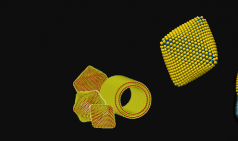
Not less important are the questions of how unique are the properties of these nanoparticles in comparison to the macroscopic materials. For example, using density functional theory, Seifert et.al., (Phys. Rev. Lett. 85, 146, (2000)), showed that the bandgap of MoS2 and WS2 nanotubes is reduced with shrinking nanotube diameter. This result is counterintuitive in comparison to semiconductor quantum dots, in which the bandgap increases with shrinking diameter. Also, in contrast to the bulk material, the bandgap of zig-zag nanotubes was predicted to be a direct one offering them potentially interesting optoelectronic behavior. Indeed using optical measurements (No. 124), and scanning probe microscopy (No. 169) of IF-WS2, we have reached similar conclusions. Recently, the extinction and absorption spectrum of suspensions of WS2 nanotubes were studied (No. 350). The nanotubes were shown to exhibit a strong light-matter interaction and act like quasi 1-D polaritonic nano-systems sustaining both the excitonic features and cavity modes in the visible-near infrared range (Fig. 11). This work was done in collaboration with Prof. Dan Oron from the Weizmann Institute; Prof. E.A. Goodilin and A.A. Fedyanin from Moscow State University and Prof. T. Ellenbogen from Tel-Aviv University.
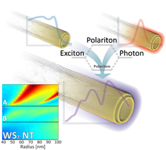
Fig. 11. Schematic illustration of the strong coupling and hybridization of modes in the nanotubes (No. 350)
The mechanical measurements of individual WS2 nanotubes were carried out and compared with ab-initio calculations (see for example Ref. 206 and 281). These works were performed in collaboration with Prof. H.D. Wagner from the Weizmann Institute and Prof. D. Golberg from NIMS, Japan. The high strength of the nanotubes (up to 20 GPa) and their elongation (12%) are compatible with their structural perfectness (see attached movies). This series of studies are indicative of their numerous applications, e.g. in ultra-high strength nanocomposites. Indeed, numerous experiments by us and others confirmed the favorable influence of minute amounts of the IF-WS2 nanoparticles and WS2 nanotubes on the mechanical and tribological properties of thermoplastic and thermosetting polymers (see for example No. 188, 245 and 252). These works were done in collaboration with Profs. Hanna Dodiuk and S. Kenig of Shenkar College. These findings have not remained in the realm of the academia only and the first product based on epoxy reinforced mechanical parts has been recently commercialized (https://www.utausa.com/).
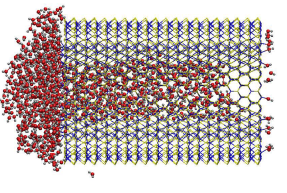
The withdrawal of single nanotube from water surface was investigated (No. 326 and Fig. 12). Importantly, nanotubes with diameter below 40 nm exhibited strong traction force from the water surface which was attributed to capillary aspiration of water molecules into the hollow core of the open-ended nanotubes. This work was carried out in collaboration with Prof. H.D. Wagner of the Weizmann Institute and Dr. A.N. Enyashin from the Russian Academy of Sciences, Ekaterinburg.
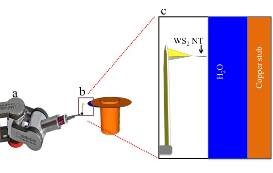
(Fig. 12.a)
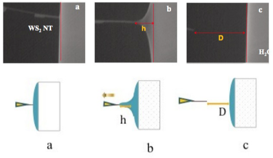
(Fig. 12.b)
(Fig. 12.c)
Fig. 12. Measurement of the traction force of WS2 nanotubes receding from water surface. a. Experimental set-up within the ESEM; b. Snapshots from the ESEM of the nanotube withdrawal from the water surface; c. Depiction of the MD simulation of the capillary soaking of water molecules into the hollow core of the WS2 nanotube (No. 326).
The electrical, electromechanical and optoelectronic properties of individual nanotubes have been investigated in recent years by us as well as by other groups. Jointly with Prof. E. Joselevich, field-effect transistors based on WS2 nanotubes with mobilities of up to 50 cm2 V−1 s−1 and high current-carrying capacity of over 0.6 mA (2.4 × 10⁸ A cm−2) were demonstrated (No. 291, see Fig. 13). More recently, electromechanical resonators based on individual WS2 nanotubes were realized in collaboration with Prof. E. Joselevich, Weizmann Institute and Dr. A. Ya’akobovitz, Ben-Gurion University, Beer Seva (No. 332)
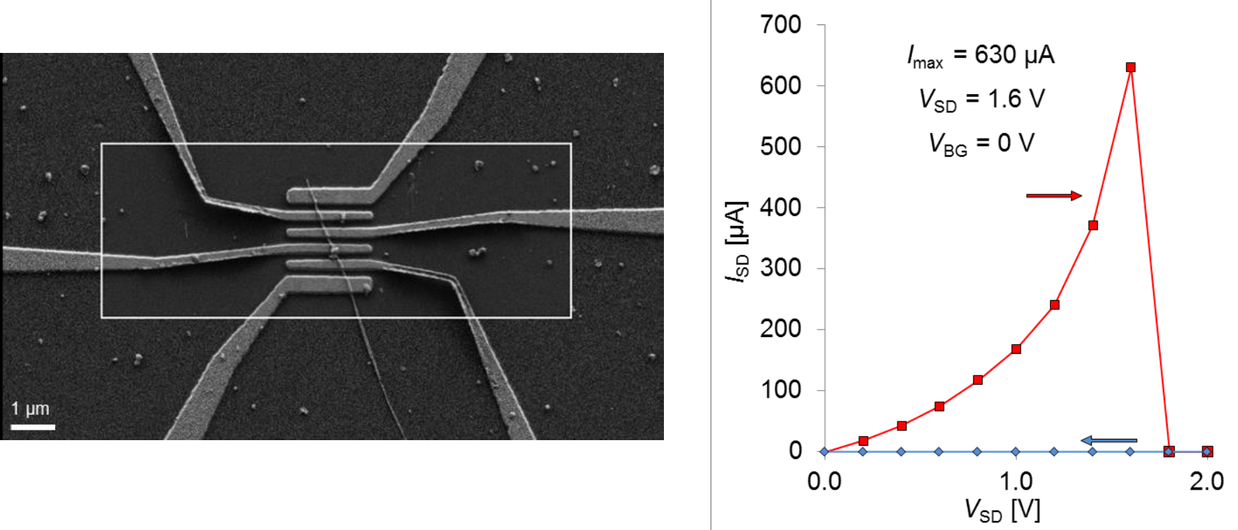
Fig. 13. SEM image of a 6-contact transistor with WS2 nanotubes (left) and I-V curve of one such transistor (right)- No. 291.
In a series of works jointly with the group of Y. Iwasa of the University of Tokyo and Riken Institute and Prof. A. Zak- Holon Institute of Technology, the low temperature transport properties of FET devices based on single WS2 tubes and ionic gating, were investigated (Fig. 14). The biased nanotube became superconductor at 5.2 K. Furthermore, Little-Parks current oscillations occurred when a magnetic field was applied parallel to the nanotube axis (No. 328). These oscillations indicated that the nanotube is an interference device with the Cooper pairs flowing on the nanotube surface in a spiral trajectory, dictated by the chirality of the nanotube. This work demonstrated the quasi-1D nature of the supercurrent in this device. In a later work (submitted), the transition temperature- Tc of the device was shown to drop with the diameter of the nanotubes, which again emphasizes the quasi-1D nature of the superconductivity in WS2 nanotubes.
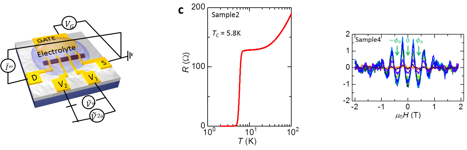
Fig. 14. Demonstration of superconductivity in WS2 nanotube: a. Schematic representation of a device with ionic liquid gate; b. Low temperature I-V curve exhibiting the transition to superconductor at 5.2 K; 3. Little-Parks oscillation of the current with magnetic field applies parallel to the tube axis. (No. 328 and 351)
In another series of works of the same groups jointly with Prof. J. Smet of the Max Planck Institute for Solid State Research, Stuttgart, the optoelectronic properties of WS2 nanotubes were investigated. In one work (No. 346), a p-n junction was realized using a single WS2 nanotube and ionic gate (Fig. 15). Light-emitting diode (electroluminescence- EL) operation and photovoltaic behavior were clearly observed. Both the emitted light and the photovoltaic device exhibited strong linear polarization characteristics due to the quasi-1D nature of the nanotube.
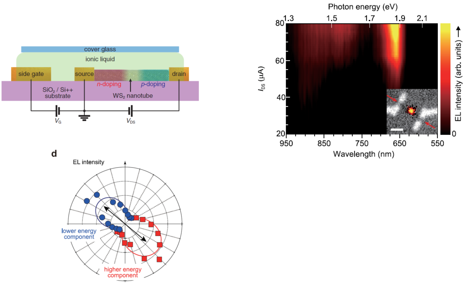
Fig. 15. Light emitting device based on a p-n junction of a single WS2 nanotube. a. Schematics of the device with ionic liquid gating; b. Spectral distribution of the EL and optical image of the light source in the inset; c. Polarization of the light emission from the nanotube device. (No. 346)
In another recent work published in Nature (No. 354), the spatial distribution of the photovoltaic (PV) effect of individual nanotube was measured and compared to that of a single and double layer WS2, using a focused laser light excitation. It was found (see Fig. 16) that, while the single and double layer WS2 show the largest PV effect near the gold contacts, the nanotube exhibits large PV effect in the center of the tube. This bulk (non-conventional) photovoltaic effect (BPVE) was attributed to the non-centrosymmetric and chiral nature of the multiwall WS2 nanotube. The BPVE exhibited by the WS2 nanotubes was some two orders of magnitudes larger than previous BPVE materials. Theoretically, the solar to electrical conversion efficiency of BPVE devices is not restricted by the Shockley-Queisser limit. Practically though, the efficiencies exhibited so far by PPVE devices (< 1%) are a far cry from the best Si photovoltaic devices.
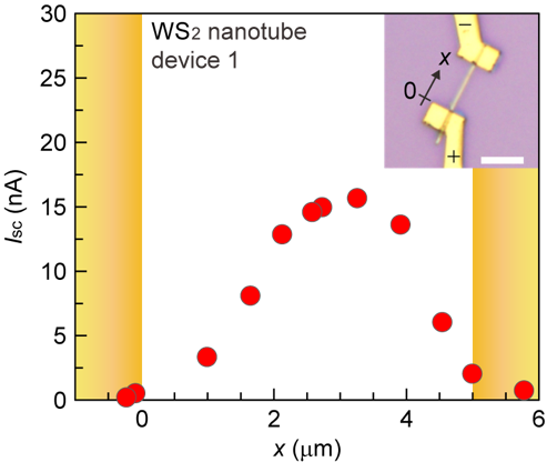
Fig. 16. Dependence of the photocurrent on laser spot position (red circles). Inset shows the nanotube with two gold contacts at the edges (No. 354).